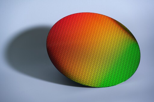
For someone more in tune with the process, honest question: how is this not a failure on ASML, who makes the lithography machines? Or the company who makes the ultra pure silicon wafers? Is Intel just feeding unetchable garbage into the machines?
Bad craftsmen always blame their tools
I think there’s more to it - IIRC, this is Intel’s factory
Things that can mess up a batch- clean room not clean enough, vibrations from walking/vehicles/tectonic activity/lack of mechanical precision, temperature variations, impurities in chemicals or wafers, em interference, static charges, etc
We’re talking a few dozen atoms in the wrong place, the tolerances are minuscule when you’re making modern chips. A small problem in the supply chain, process, or the building itself could all kill your yield
I’m not an expert or anything, but I know this is a very unforgiving field
Never thought I’d see the absolute downfall of Intel in my lifetime but the last decade has not been good for them.
To be fair, they sat on their hands for a fair amount of it.
I was curious how bad 10% was, so I went digging to see what it should be.
A “good” yield target on a modern process is something like 60-70%, so this is a shocking shockingly bad oof, though it’s also not a complete process, so it’s possible they can salvage this and turn it into something viable but, still, oof.
That wafer be lookin’ like a delicious mango in the thumbnail. 🤤
Does this A in 18A stand for ångström? Can they even produce anything below 10 nm?
Yes, it does. It’s ambitious and a real stretch for Intel. But some are doubting this story of the yields being so low:


